Inverter PCB Modeling
Introduction
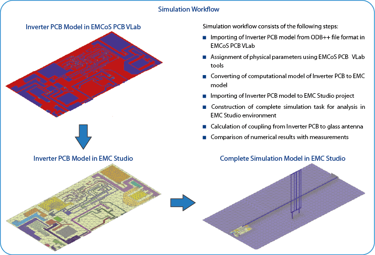
This document demonstrates modeling of Printed Circuit Boards (PCB) with Green Function approach using new powerful tools of EMCoS PCB VLab and EMC Studio. In conjunction, these two products make it easy to build a full simulation chain for various types of PCB models. This application note considers case of power Inverter PCB and its coupling to glass antenna. The obtained results are compared to laboratory measurements.
Simulation Workflow
Measurement Setup
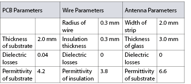
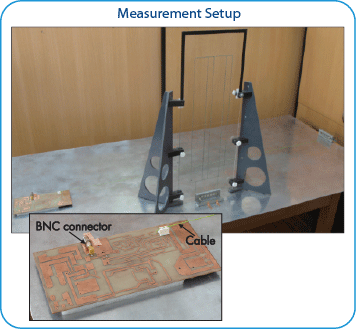
Measurement setup contains single wire connected to Inverter PCB and glass antenna located at 28 cm from cable. Parameters components of setup are listed in table below.
Measurements of coupling from Inverter PCB were performed in EMCoS laboratory.
Results
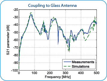
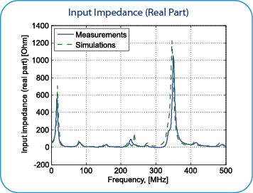
The comparison of simulation and measurement results is shown below. There is good agreement between measurement and simulation results in considered frequency range.
![]()
Calculation Efficiency
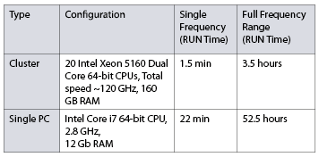
Calculations were performed on EMCoS cluster and on standalone PC. Computational time for one model calculation of 143 sample points in complete frequency range from 300 kHz to 500 MHz is shown in table.
Conclusions
According to performed investigation the main conclusions are:
- Computational model of PCB can be effectively generated using EMCoS PCB VLab and EMC Studio
- Simulation results of coupling from PCB are in good agreement with measurement results