Modeling of EMC-Filter from Würth Elektronik Design Kit
Introduction
This application note demonstrates the results of cooperation project between EMCoS Ltd. and Würth Elektronik eiSos GmbH & Co. KG. It shows different techniques for modeling of EMC filter performance assembled based on Würth Elektronik EMC-Filter Design Kit in EMCoS Studio environment. Depending on initial data availability, either circuit simulation approach, or 3D fullwave simulation can be applied. The EMCoS Studio software package supports all required tools to perform accurate modelling of filter components and fast assembling of filter models.
Simulation Model Description
The filter samples and corresponding simulation models were constructed using passive components and evaluation board from Würth Elektronik EMC-Filter Design Kit 744 998.
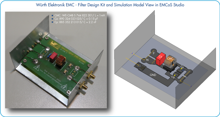
Modeling of the WE Components for Fullwave and Circuit Simulations
Filter components used for assembling of filter model can be modeled in EMCoS Studio environment in different ways depending on the chosen simulation method (circuit or 3D MoM fullwave analysis). In circuit simulations, filter components can be defined either as circuit elements with nominal values and stray parameters included in the circuit element definition or based on measured/simulated S-parameters. For 3D MoM fullwave simulations filter components should be modeled as voluminous objects with corresponding frequency-dependent material parameters.
In this application note we constructed 3D models of the filter components, calculated their S-parameters with fullwave MoM solver and used them in circuit simulation. All filter components used in the model construction are available in the integrated Filter Components Library.
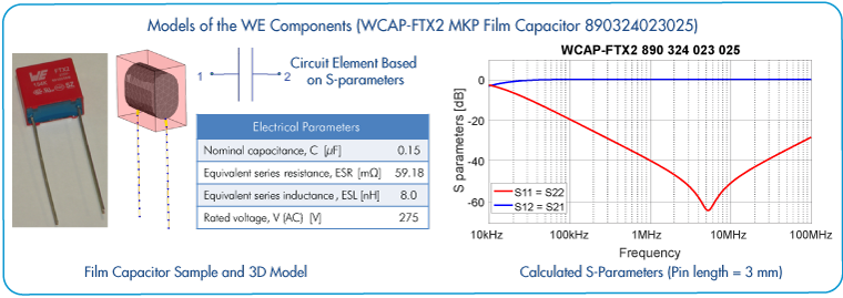
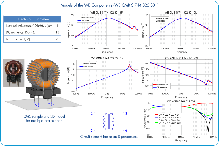
Below are presented models for film capacitor (WCAP-FTX2 MKP Film Capacitor 890324023025) and toroidal choke (WE-CMB S 744 822 301) with calculated S-data:
Validation of the constructed 3D model of the toroidal choke shows good agreement between simulated and measured results:
Circuit Simulations with Filter Components Based on S-Parameters
This part of the application note demonstrates circuit simulation of the filter model with components based on simulated/measured S-parameters. Simulations are performed with TSReady, mixed S-parameters/circuit solver, included in EMCoS Studio package.
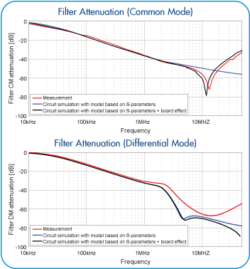
Figures presented below illustrate filter attenuation for common and differential mode disturbances:
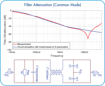
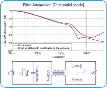
The discrepancy between measured and simulated results for upper frequency range can be explained by the fact that the contribution of stray elements introduced by PCB layout is not considered in the circuit model of the filter.
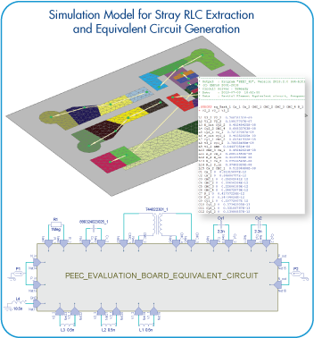
Modeling of PCB Layout Effect with 3D PEEC Solver
This section presents a methodology for investigation of the filter performance by examining the impact of stray parameters of printed circuit board (PCB). First, stray parameters are extracted from the board layout using 3D quasistatic field solvers. Second, the corresponding equivalent circuit is constructed. Third, the extracted equivalent circuit is combined with functional circuit of the filter.
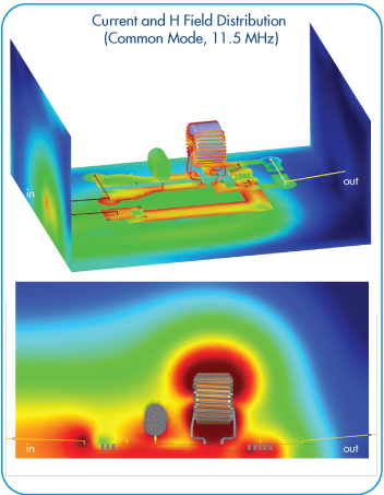
The 3D model of filter evaluation board with assigned branches and ports is shown below. This model is constructed to extract stray capacitances and inductances from metallic structures and to add them to the functional schematic, thus, taking into account the impact of the actual board layout. Resonance of common mode attenuation at 11 MHz is caused by the inductance value of the grounding trace (GND) of the evaluation board. Simulation model takes into account this effect and also shows resonance behaviour.
3D Simulations with Fullwave MoM Solver
The comparison of fullwave results with circuit simulations, including filter components based on S-parameters and equivalent circuit of PCB layout is shown below:
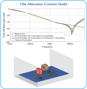
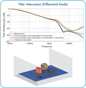
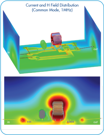
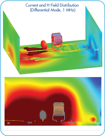
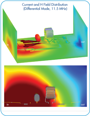
The simulated 3D fullwave results are in better agreement with measured results for differential mode attenuation in the upper frequency range. This can be explained by the fact that 3D fullwave model accounts for 3D field coupling effect between the voluminous components of the filter. In case of common mode attenuation both approaches give practically the same results due to the interactions defined by the conductive effects of the PCB traces. The described effects can be clearly seen from the 3D current and field distribution plots:
Application note was prepared in cooperation with Würth Elektronik eiSos GmbH & Co. KG